Sidebar
<latex>{\fontsize{16pt}\selectfont \textbf{Development of a Prototype for a High Resolution Tactile Sensor}} </latex>
<latex>{\fontsize{12pt}\selectfont \textbf{Christian Bärtschi}} </latex>
<latex>{\fontsize{10pt}\selectfont \textit{Semester project ME}} </latex>
<latex> {\fontsize{12pt}\selectfont \textbf{Abstract} </latex>
In this project we develop the prototype of a high resolution tactile sensor for micro-wear analysis in archeology. In the experimental part of micro-wear analysis, mechanical interaction between the stone and the underground causes abrasive effects on the microscopic scale. In order to correlate measurements of the degree of wear taken on areas of sub-mm size with macroscopic parameters of the experiment like force and duration, the contact pressure on the area of interest must be known. To overcome this problem we want to measure the pressure distribution of the stone surface during contact, using a high resolution tactile sensor.
The sensor we plan to use for this task relies on the principle of optical tactile sensing, or more specifically on frustrated total internal reflection (FTIR). To create a working sensor prototype a mechanical setup incorporating all essential sensor components was designed and constructed. Further, we fabricated a structured silicon rubber membrane which serves as the main transducer, using conventional MEMS processing techniques and PDMS casting. Finally, an image processing procedure able to automatically convert the raw image data from the sensor to an array of output values was succesfully implemented.
<latex> {\fontsize{12pt}\selectfont \textbf{Tactile Sensing} </latex>
Tactile sensors are devices which try to mimic the human sense of touch. In other words: They measure effects caused by physical interaction, like contact force or temperature. Tactile sensing is used in everyday appliances like buttons and touchscreens, but it is also important in current research, as for example in robotic perception and manipulation. 1)
Most tactile sensors consist of an array of multiple pressure or force transducers, so called tactile cells or taxels. This makes them capable of not only measuring the amount of force applied but also gather spatial information. This spacial information is very important and its subsequent interpretation useful for many applications.
Many different physical effects can be used to build touch sensing arrays. Capacitive and resistive sensing arrays are widley used but also acoustic and magnetic tactile sensors were succesfully implemented.
A major drawback of most tactile sensor designs are the complicated fabrication and the intricate control circuits required for big arrays. To create a high resolution tactile sensor without the need of extensive MEMS processing or complex circuitry we decide to use optical tactile sensing instead.
 The sensor we use for our application relies on the principle of frustrated total internal reflection (FTIR). By placing a structured rubber membrane on top of a plate of transparent material, flooded with light, we can observe the contact pattern from underneath. The membrane consists of a thin silicone sheet with a grid of very fine, pyramid shaped protrusions, so called taxels. When force is applied to the back of the membrane, the taxels are pressed against the waveguide, causing them to flatten with the contact area being a function of the force per taxel. Coupled with the effect of FTIR which causes the light to scatter where the membrane touches the plate, this creates a transducer from contact forces to light intensity and pattern. The light can then be captured using a conventional digital camera and subsequent image processing.
<latex> {\fontsize{12pt}\selectfont \textbf{Sensor Design} </latex>
To use the principle of optical tactile sensing for our application, we need to design a mechanical setup which incorporates the sensing membrane, an illuminated waveguide and a way of capturing images of the scattered light.

The general design of our sensor has the form of a small table with a transparent top, serving as waveguide, and an integrated light source. On top of the transparent surface lies the structured rubber sensing membrane. Underneath the table is a mounted camera, used to capture pictures of the contacting pattern.
This setup allows us to measure the pressure distribution on the contact area of a sample by placing it on the sensing membrane and applying the desired force. We then take a picture with the camera and extract the data using image processing.
The body of the sensor is constructed to consist mainly of patterned plates and tubes for ease of fabrication and replication using a laser-cutter.
The waveguide consists of a 15cm by 15cm square of acrylic glass (PMMA) with a thickness of 4mm. A layer of reflective aluminium tape is applied to three edges to contain the light inside the plate. The remaining side is left clear to allow light to enter the waveguide.
In advance all four sides had to be carefully sanded and polished to ensure optimal optical properties.
As material for the waveguide we tested acrylic (PMMA) as well as lexan (polycarbonate). Both materials are clear thermoplastics with similar optical properties. Polycarbonate would be favorable because of its higher stiffness and strength as well as its chemical resistance. Despite these advantages, acrylic proved to be better suited as it produces a much brighter contact pattern. This difference seems to be caused mainly by the quality of the edge finish. Other than polycarbonate, acrylic can be flame polished resulting in a much cleaner surface than polishing by hand. Because of this, the polycarbonate ends up with “darker” edges, causing more light to be lost when entering the plate or reflecting off the sides.|
For the integrated light source we use an array of 25 bright, green LEDs with a luminosity of 59'000 mcd and a radiation angle of 15 degrees. The LEDs were soldered to a piece of veroboard, each in series with a current limiting resistor, and connected to a 5V power source. The single color LEDs allow to concentrate the signal to one color channel in the camera image which simplifies image processing and further enhances signal to noise ratio.
The camera used is a Nikon D3300 with an AF-S Micro NIKKOR 60mm f/2.8G~ED macro lens. The camera is mounted vertically on a rail beneath the center of the waveguide, using a quick release system.
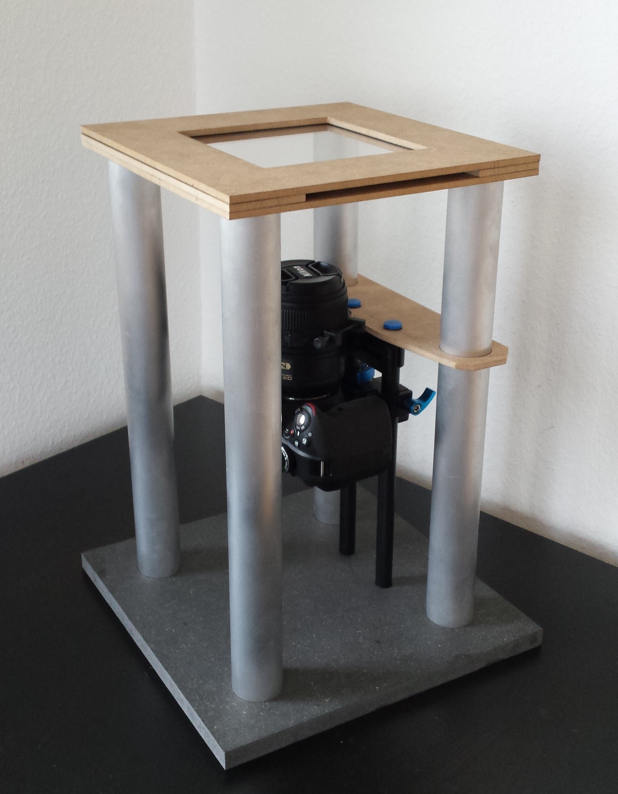 Finished setup | 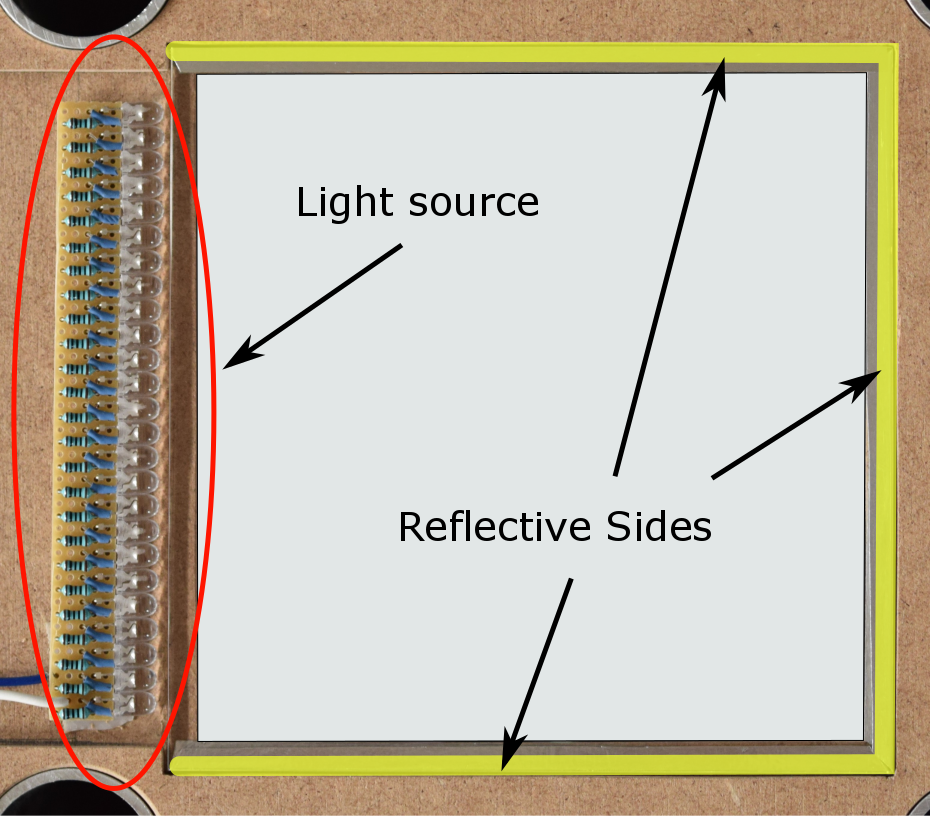 Detailview of the waveguide and integrated light source |
<latex> {\fontsize{12pt}\selectfont \textbf{Sensing Membrane} </latex>
The rubber sensing membrane is the most important part of the optical tactile sensor. It consists of a thin sheet of opaque, cross-linked polydimethylsiloxane (PDMS), a widely used silicone elastomer. The membrane's surface is patterned with an array of small spikes, so called taxels, which serve as the main transducer from pressure to contact area. The exact transducer characteristics depend on how the taxels deform and are a combination of the material properties and the taxel geometry.
Each taxel has the shape of a truncated pyramid with a quadratic footprint and a slope of ~35.3°, predefined by the fabrication process.

For the fabrication of the sensing membrane, we first create a mold from a silicon wafer by etching a grid of pyramid shaped depressions in its surface (a). Afterwards, the PDMS rubber is cast onto the wafer (b), cured in an oven and demolded © to obtain the sensing membrane.
<latex> {\fontsize{12pt}\selectfont \textbf{Image Processing} </latex>
With the mechanical setup and the membrane finished, we are able to probe first samples and take pictures of the taxels' contacting pattern.
To create a meaningful output from these pictures, the data must be extracted using image analysis.
The main metric we are interested in, is the contact area of each taxel, which we need to determine automatically and write to an output file.

Due to the frustrated total internal reflection where the membrane touches the waveguide, we expect high contrast between contacting points and the background.
This difference in intensity allows us to segment the image using simple thresholding.
We chose a threshold value slightly above the average intensity.
All pixels with an intensity higher or equal to the threshold are classified as “object” and assigned the value 1, the pixels with an intensity below the threshold are background and set to 0.
If the thresholding value is set right, this results in a bicolour image with the contacting areas separated from the background.
Because the sensing membrane is not fixed to the waveguide or with respect to the camera, we have to find its orientation and rotate the image to align the taxel grid.
To find the orientation we search for straight lines in the pictures, representing rows of taxels. This line extraction is done by calculating and analyzing the Hough transform of the image.
Hough space is the parameter space of all possible lines contained in an image. By using the line parametrization $$x\cos{\theta}+y\sin{\theta}=\rho$$ we can express all straight lines by their angle ($\theta$) and distance from the origin ($\rho$).

When calculating the Hough transform of our segmented pictures, we can see multiple peaks located at certain angles. These peaks represent the rows or columns of our taxel grid and the angles at which they occur correspond to orientation of our membrane.
To determine the spacing of the taxel grid we use frequency analysis. Due to the very regular, periodic pattern of the membrane we can expect to find strong corresponding peaks in the power spectrum of our image. To analyze the power spectrum, we decompose the image into its frequency components using the discrete Fourier transform. Since the image is already aligned correctly, we only need to find frequency components in vertical and horizontal direction. This allows us to calculate the row and column sum vectors of our image and analyze them, rather than the full picture. Employing this technique reduces the amount of data significantly, while preserving all relevant information for this step. By locating the frequency with the highest magnitude and calculating the associated period, we get a good estimate of the grid spacing.

<latex> {\fontsize{12pt}\selectfont \textbf{Results and Discussion} </latex>
The sensor prototype developed in this paper demonstrates a successful proof-of-concept of an optical high resolution tactile sensor, based on the principle of frustrated total internal reflection.
We designed a mechanical setup incorporating all the essential components and identified the critical sensor parameters.
Multiple sensing membranes, with different taxel parameters, and the necessary corresponding silicon molds were fabricated.
Using our setup, we successfully took sample pictures and implemented a robust image processing procedure, able to automatically determine the contact area of each taxel and writing it to an output file.
As can be seen in the sample pictures our prototype is already able to pick up the pressure difference caused by small surface irregularities.

Page Tools
